q Epitaxy & CVD | ALD / ALE | More than Moore | Custom Evaporators
Enabling next generation devices
Thin Film processing on the scale of single atomic layers is gaining growing interest with the increasing demand of modern structures in microelectronics. Multiple patterning with Atomic Layer Deposition ALD, the deposition of high-k films like Al2O3 and Zr/Hf Oxides or 3D structures are key processes for technology milestones beyond 10 nm in logic and memory.
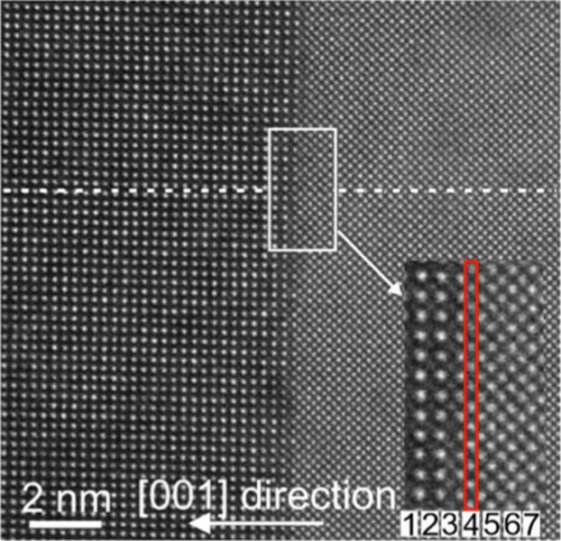 | Enabling hetero-abrupt semiconductor interfaces by precise control of precursor flows. (© picture courtesy of University Marburg) |
However, ALD is also attracting a lot of attention outside the silicon based microelectronics world. It is used to coat float glasses or is applied to even create even complex 3D structures with highest precision.
As described above, modern nano-electronics require precision on nanometer scale and control on atomic layer level. Besides the deposition of materials, one of the most important challenges for further downscaling of CMOS circuits is precise etching on atomic scale. Atomic Layer Etching (ALE) offers the unique opportunity to etch with atomic precision and minimal material destruction (component damage). This will enable structural dimensions smaller than 3 nm.
ALD and ALE chemicals so called Precursors are often toxic, pyrophoric and corrosive – or a combination of all of them. Therefore many users still hesitate to apply them in production as safety concerns are not addressed entierely. Also ALE and ALD systems have to be synchronized exactly to work precisely and efficiently.
Therefore SEMPA SYSTEMS develops and optimizes highest speed gas feeding solutions for efficient ALD/ALE systems. We do also address important safety aspects in our CHEM'BOT family of supply system (especially in combination with LCAS for energetic materials).
For SEMPA ALD/ALE are processes with huge potentials. We work here in cooperation projects like ALP (Atomic Layer Processing) and ATOPLOT (Atomic Layer 3D Plotter).
SEMPA SYSTEMS GmbH
Grenzstraße 13
01109 Dresden
Germany
![]() +49 (0)351-888 10 0
+49 (0)351-888 10 0 ![]() +49 (0) 351-888 10 15
+49 (0) 351-888 10 15
x sales (hello@spam.com) sempa.de
SEMPA SYSTEMS GmbH | Grenzstraße 13 | 01109 Dresden | Germany
+49 (0) 351 888 10 0 | info (hello@spam.com) sempa.de
© 2023 by SEMPA SYSTEMS | german certified manufacturer of high precision equipment